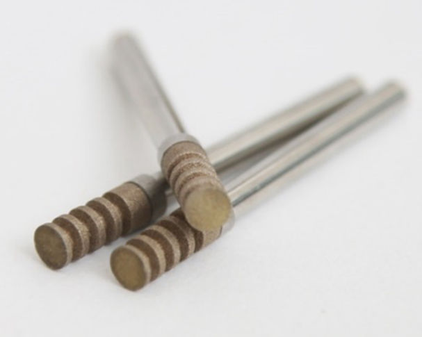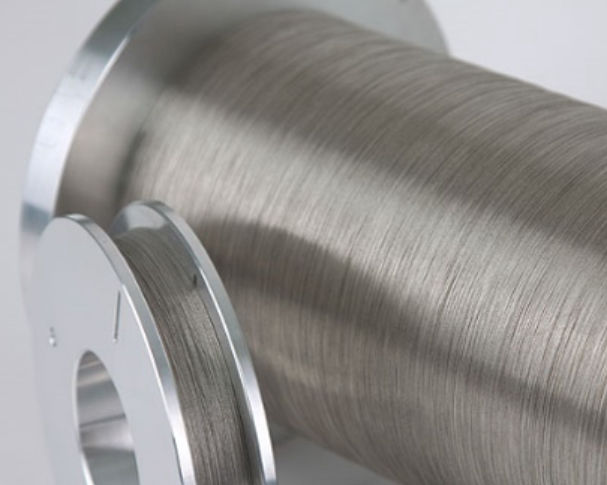
Diamond Wire (LED, Solar, Glass, Ceramic)
High throughput & Superior cutting quality
- Reduced process lead time and kerf loss
- Enhanced flatness of cut materials and superior warp, TTV and Bow values
• Applicable for thin wafer slicing – Through uniform diamond grit
• Longer wire lifetime – Excellent diamond retention & no wire breakage
• Faster cutting speed – 3~10 times compared with slurry process
• Low cost and eco-friendly – Slurry free process
• EHWA & MWEDC
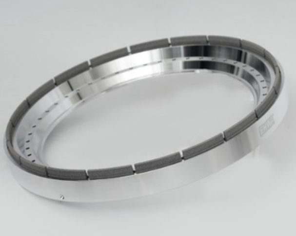
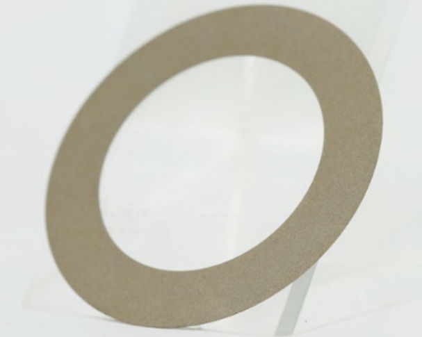
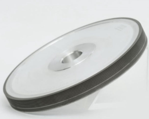
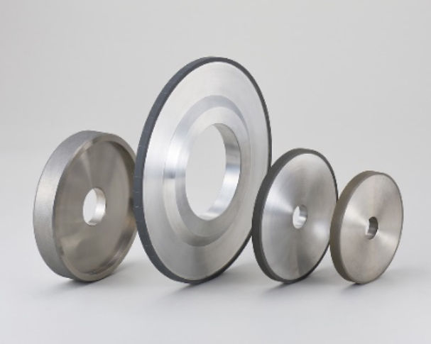
EHWA Back Grind Wheel (Vitrified & Resin)
• Wafer surface roughness and die strength can be improved
• Grinding stress and wafer edge chipping can be reduced
• Diamond at the tip can be distributed consistently
• Porosity, pore shape and pore size control can be adjusted
• Possible to grind Si wafer up to 17㎛ (Ultra thin wafer)
• Outstanding grinding ability for TSV and normal(for finger print) compound wafer
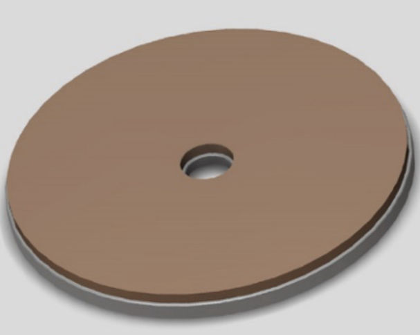
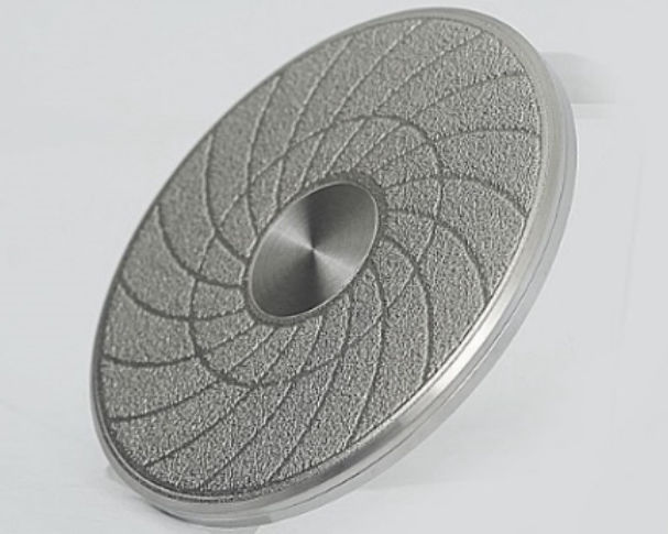
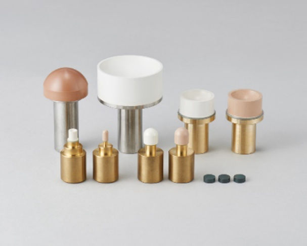
EHWA DP Wheel
• Applying dry polishing after processing wafer with back grinding wheel.
• Mirror surface processing by using soft wool felt and ZrO2 250mm for improving
roughness.